- 您现在的位置:买卖IC网 > Sheet目录317 > C8051T610DB24 (Silicon Laboratories Inc)DAUGHTER BOARD T610 24QFN SOCKET
�� �
�
�C8051T610/1/2/3/4/5/6/7�
�22.5.� SMBus� Transfer� Modes�
�The� SMBus� interface� may� be� configured� to� operate� as� master� and/or� slave.� At� any� particular� time,� it� will� be�
�operating� in� one� of� the� following� four� modes:� Master� Transmitter,� Master� Receiver,� Slave� Transmitter,� or�
�Slave� Receiver.� The� SMBus� interface� enters� Master� Mode� any� time� a� START� is� generated,� and� remains� in�
�Master� Mode� until� it� loses� an� arbitration� or� generates� a� STOP.� An� SMBus� interrupt� is� generated� at� the� end�
�of� all� SMBus� byte� frames.� As� a� receiver,� the� interrupt� for� an� ACK� occurs� before� the� ACK.� As� a� transmitter,�
�interrupts� occur� after� the� ACK.�
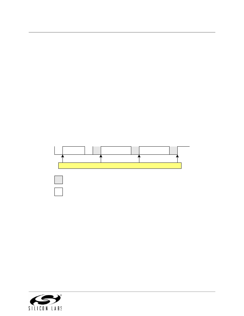
�22.5.1.� Write� Sequence� (Master)�
�During� a� write� sequence,� an� SMBus� master� writes� data� to� a� slave� device.� The� master� in� this� transfer� will� be�
�a� transmitter� during� the� address� byte,� and� a� transmitter� during� all� data� bytes.� The� SMBus� interface� gener-�
�ates� the� START� condition� and� transmits� the� first� byte� containing� the� address� of� the� target� slave� and� the�
�data� direction� bit.� In� this� case� the� data� direction� bit� (R/W)� will� be� logic� 0� (WRITE).� The� master� then� trans-�
�mits� one� or� more� bytes� of� serial� data.� After� each� byte� is� transmitted,� an� acknowledge� bit� is� generated� by�
�the� slave.� The� transfer� is� ended� when� the� STO� bit� is� set� and� a� STOP� is� generated.� Note� that� the� interface�
�will� switch� to� Master� Receiver� Mode� if� SMB0DAT� is� not� written� following� a� Master� Transmitter� interrupt.�
�Figure� 22.5� shows� a� typical� master� write� sequence.� Two� transmit� data� bytes� are� shown,� though� any� num-�
�ber� of� bytes� may� be� transmitted.� Notice� that� all� of� the� “data� byte� transferred”� interrupts� occur� after� the� ACK�
�cycle� in� this� mode.�
�S�
�SLA�
�W�
�A�
�Data� Byte�
�A�
�Data� Byte�
�A�
�P�
�Interrupt� Locations�
�Received� by� SMBus�
�Interface�
�Transmitted� by�
�SMBus� Interface�
�S� =� START�
�P� =� STOP�
�A� =� ACK�
�W� =� WRITE�
�SLA� =� Slave� Address�
�Figure� 22.5.� Typical� Master� Write� Sequence�
�Rev� 1.1�
�143�
�发布紧急采购,3分钟左右您将得到回复。
相关PDF资料
C8051T630DB20
BOARD SOCKET DAUGHTER 20-QFN
CAN-100
BOARD EVAL RS232 100QFP
CANADAPT28
KIT ADAPTER CANDEMOBOARD 28PLCC
CAT24AA01WI-GT3
IC EEPROM SERIAL 1KB I2C 8SOIC
CAT24AA02WI-G
IC EEPROM SERIAL 2KB I2C 8SOIC
CAT24C01ZI-G
IC EEPROM SERIAL 1KB I2C 8MSOP
CAT24C03WI-G
IC EEPROM SERIAL 2KB I2C 8SOIC
CAT24C04ZI-G
IC EEPROM SERIAL 4KB I2C 8MSOP
相关代理商/技术参数
C8051T610DB28
功能描述:子卡和OEM板 C8051T610 Family Socket Daughtr Board RoHS:否 制造商:BeagleBoard by CircuitCo 产品:BeagleBone LCD4 Boards 用于:BeagleBone - BB-Bone - Open Source Development Kit
C8051T610DB32
功能描述:子卡和OEM板 C8051T610 Family Socket Daughtr Board RoHS:否 制造商:BeagleBoard by CircuitCo 产品:BeagleBone LCD4 Boards 用于:BeagleBone - BB-Bone - Open Source Development Kit
C8051T610DK
功能描述:开发板和工具包 - 8051 C8051T610 Series Development Kit RoHS:否 制造商:Silicon Labs 产品:Development Kits 工具用于评估:C8051F960, Si7005 核心: 接口类型:USB 工作电源电压:
C8051T610-GQ
功能描述:8位微控制器 -MCU 16KB 10ADC 32Pin MCU RoHS:否 制造商:Silicon Labs 核心:8051 处理器系列:C8051F39x 数据总线宽度:8 bit 最大时钟频率:50 MHz 程序存储器大小:16 KB 数据 RAM 大小:1 KB 片上 ADC:Yes 工作电源电压:1.8 V to 3.6 V 工作温度范围:- 40 C to + 105 C 封装 / 箱体:QFN-20 安装风格:SMD/SMT
C8051T610-GQR
功能描述:8位微控制器 -MCU 16KB 10ADC 32Pin MCU RoHS:否 制造商:Silicon Labs 核心:8051 处理器系列:C8051F39x 数据总线宽度:8 bit 最大时钟频率:50 MHz 程序存储器大小:16 KB 数据 RAM 大小:1 KB 片上 ADC:Yes 工作电源电压:1.8 V to 3.6 V 工作温度范围:- 40 C to + 105 C 封装 / 箱体:QFN-20 安装风格:SMD/SMT
C8051T611-GM
功能描述:8位微控制器 -MCU 16KB 10ADC 28Pin MCU RoHS:否 制造商:Silicon Labs 核心:8051 处理器系列:C8051F39x 数据总线宽度:8 bit 最大时钟频率:50 MHz 程序存储器大小:16 KB 数据 RAM 大小:1 KB 片上 ADC:Yes 工作电源电压:1.8 V to 3.6 V 工作温度范围:- 40 C to + 105 C 封装 / 箱体:QFN-20 安装风格:SMD/SMT
C8051T611-GMR
功能描述:8位微控制器 -MCU 16KB 10ADC 28Pin MCU RoHS:否 制造商:Silicon Labs 核心:8051 处理器系列:C8051F39x 数据总线宽度:8 bit 最大时钟频率:50 MHz 程序存储器大小:16 KB 数据 RAM 大小:1 KB 片上 ADC:Yes 工作电源电压:1.8 V to 3.6 V 工作温度范围:- 40 C to + 105 C 封装 / 箱体:QFN-20 安装风格:SMD/SMT
C8051T612-GQ
功能描述:8位微控制器 -MCU 8KB 10ADC 32Pin MCU RoHS:否 制造商:Silicon Labs 核心:8051 处理器系列:C8051F39x 数据总线宽度:8 bit 最大时钟频率:50 MHz 程序存储器大小:16 KB 数据 RAM 大小:1 KB 片上 ADC:Yes 工作电源电压:1.8 V to 3.6 V 工作温度范围:- 40 C to + 105 C 封装 / 箱体:QFN-20 安装风格:SMD/SMT